At Embedded World exhibition in Nuremberg, I walked past a PMK booth and stopped.
Not because of the product brochures. Because of what was on the table.
A complete GaN half-bridge switching measurement setup — live, running, with four probes simultaneously capturing the exact signals that define whether your power device behaves the way you think it does.
Most engineers who design GaN converters have never seen all four signals captured correctly at the same time. This demo showed exactly why that matters — and what it takes to do it right.

Photo: image1.png — full overview shot
Caption (italic): GaN half-bridge switching measurement setup at PMK booth · Embedded World 2026
The Four Signals You Have to Capture
GaN switching measurement comes down to four quantities. All four, simultaneously — or your characterization is incomplete:
→ HS Vgs — High-side gate voltage
→ LS Vgs — Low-side gate voltage
→ Vds — Switching node voltage (the violent one)
→ Isw — Switching current
Together, these four signals tell you: when the device actually turns on, how fast the voltage swings, whether there's shoot-through, and what the real switching loss looks like — not the simulated version.
The problem? Each of these signals creates a different measurement challenge. And GaN pushes every one of those challenges to the limit.
Why GaN Makes This Hard
Two numbers define the difficulty:
dv/dt: 50–100 V/ns
The switching node can swing 400 V in under 10 nanoseconds. Any parasitic capacitance in your probe tip — a few picofarads is enough — will inject current into that node, distort the waveform, and in extreme cases, affect the switching behavior itself.
This is the hidden trap most engineers miss: at high enough dv/dt, your probe stops being a measurement tool. It becomes part of the circuit.
di/dt: >100 A/ns
Current changes faster than most probes can track. A current clamp with 50 MHz bandwidth looks perfectly reasonable — until you realize that GaN switching events happen in the sub-nanosecond range. The result is not just a blurry waveform. It's a fundamentally wrong one.
How the PMK Demo Solves It — Probe by Probe

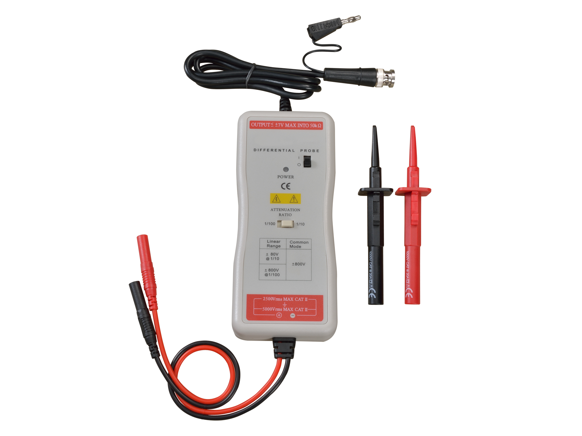
1 → FireFly® FF-1500A (PMK) — Optical Isolated Probe
Used for: Vds at the switching node
The FireFly is not a conventional differential probe. It converts the signal to digital at the tip, transmits it over optical fiber, and reconstructs it at the receiver connected to the scope. No galvanic connection between the measurement point and the oscilloscope.
Why this matters for GaN:
→ Full galvanic isolation eliminates ground loop noise
→ CMRR stays high even at 100 V/ns dv/dt — where copper-path probes fail
→ No probe capacitance loading the switching node
→ Rated for the high common-mode voltages present in half-bridge topologies
The 10:1 tip (FF-1500A configuration) extends the voltage range while keeping bandwidth usable for GaN transitions.
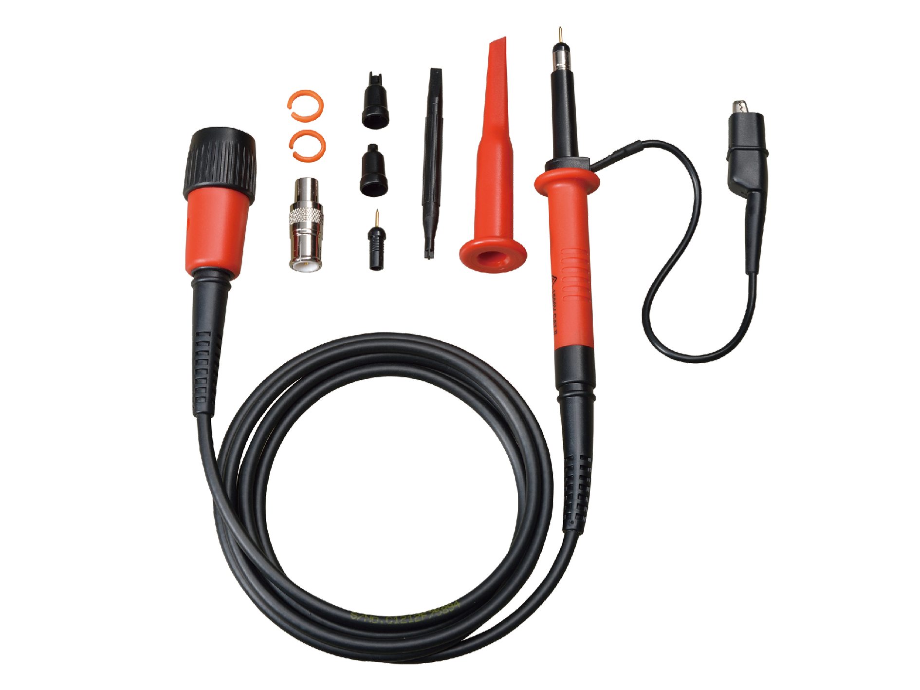
2 → High-Speed Differential Probe (HSDP)
Used for: Gate signals (HS Vgs / LS Vgs)
Gate voltages are small — typically 0 to +6 V for GaN, sometimes with a negative turn-off rail. The differential probe handles the floating reference of the high-side gate without the isolation overhead of the FireFly. Good bandwidth, low input capacitance, appropriate for the relatively benign gate signal environment.
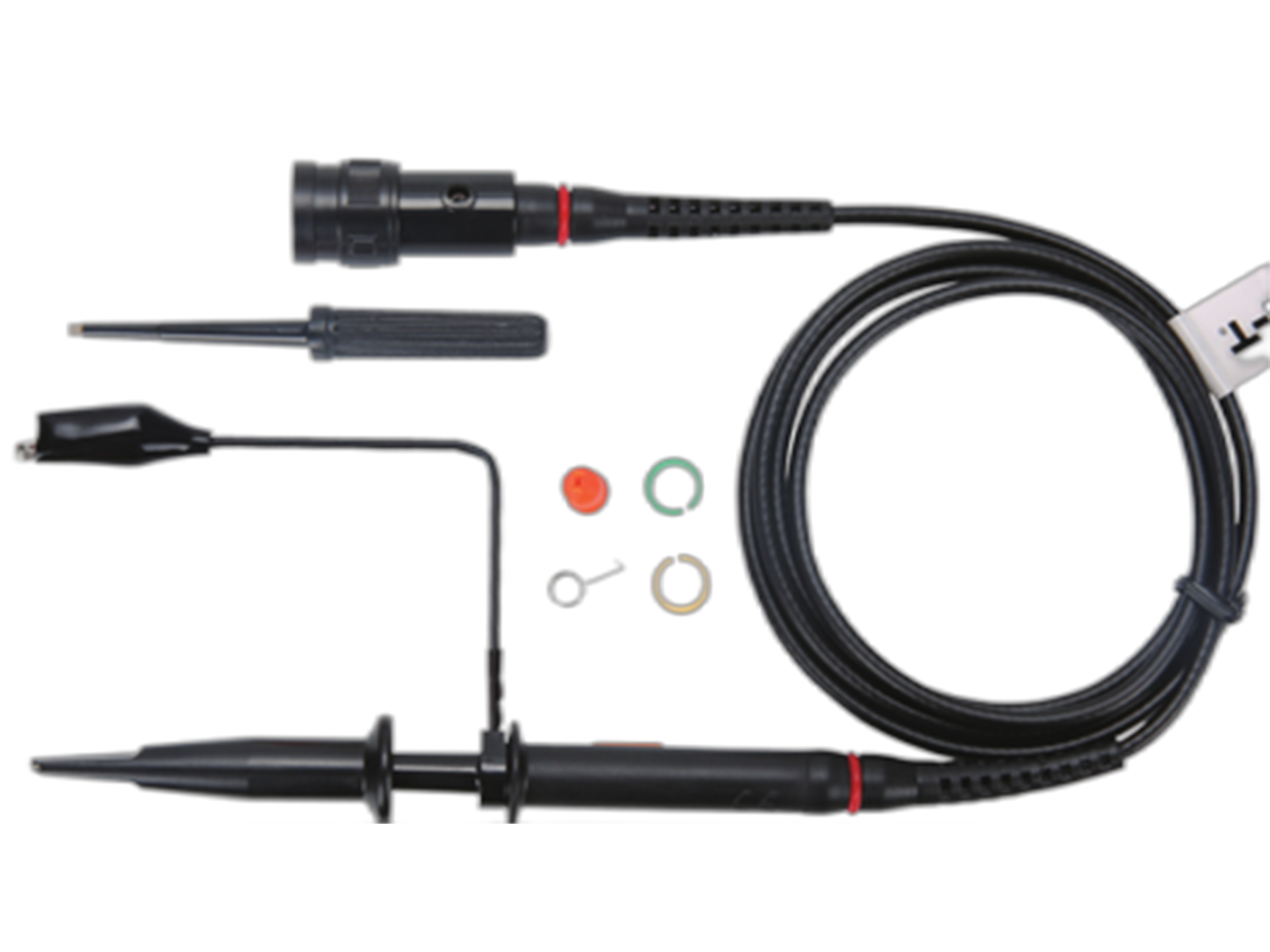
3 → MMCX Passive Probe
Used for: On-board test points
This is a detail most people overlook. The Infineon GaN demo board in this setup provides MMCX-format test points directly on the PCB. Instead of attaching a probe tip with several centimeters of ground lead, you connect with a matched impedance MMCX connector — near-zero additional inductance, no ground loop antenna.
This is not a luxury. At GaN switching speeds, even 1 cm of ground lead adds enough inductance to create ringing that looks like a real signal artifact — but is entirely a measurement artifact.
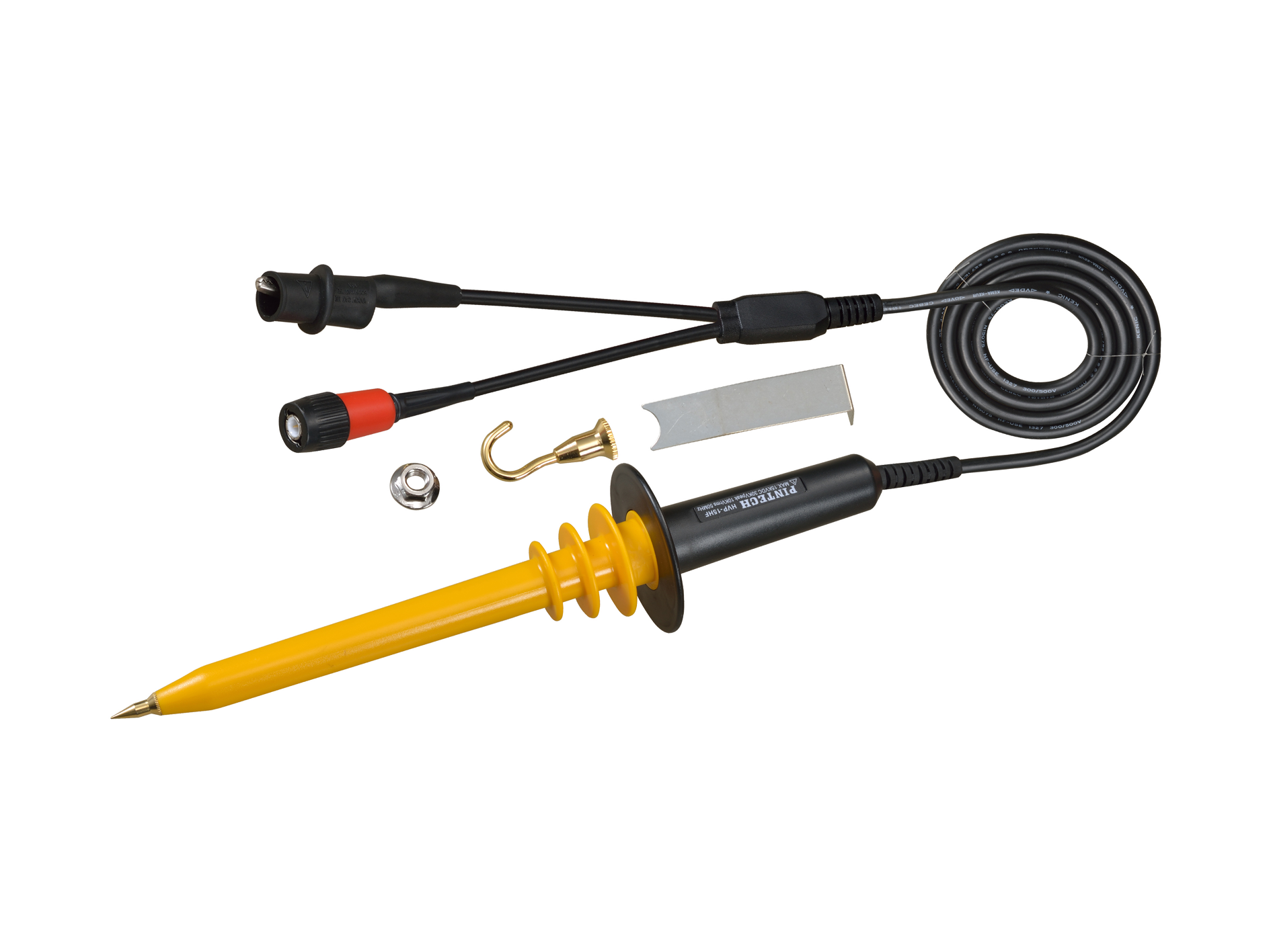
4 → UFCS Series Ultra-Fast Current Shunt (PMK)
Used for: Isw — switching current
No current clamp here. The UFCS shunt is a precision low-inductance resistor in the current path — the voltage across it, measured via the differential probe, gives you the current waveform with bandwidth that a clamp-style probe cannot match.
The key spec is inductance, not resistance. A shunt with even 1 nH of parasitic inductance will produce a voltage spike at di/dt = 100 A/ns. The UFCS series is optimized to minimize exactly this.
What the Scope Screen Shows

PMK FireFly® optical receiver unit and UFCS Ultra-Fast Current Shunt demo display · Embedded World 2026
The Iwatsu oscilloscope behind the demo board was showing four-channel simultaneous capture:
→ Yellow — Vds (switching node, the 400 V swing)
→ Pink — HS Vgs (high-side gate)
→ Cyan — LS Vgs (low-side gate)
→ Green — Isw (switching current via shunt)
What's immediately visible: the timing relationship between gate events and the switching node transition. Delay between gate drive and actual Vds swing — that's your effective dead time. Overlap between gate states — that's shoot-through risk. Current shape during turn-on — that's your switching loss.
None of this is visible if even one probe is wrong.
The Hidden Problem Most Engineers Don't Debug
Here's what doesn't show up in the datasheet or the application note:
Most GaN switching waveforms look clean. Because the probe is filtering the truth.
A conventional passive probe on a 400 V switching node at 100 V/ns dv/dt will produce a waveform. It just won't be the real waveform. The parasitic capacitance of the probe loads the node. The ground lead inductance rings. The limited CMRR of a single-ended probe couples the common-mode swing into the measured signal.
Engineers see a waveform, assume it's correct, and optimize around it. The real switching behavior — the one that determines EMI signature, device stress, and efficiency — remains unmeasured.
This is why the probe selection for GaN measurement is not a detail. It's the foundation of the characterization.
What This Demo Is Actually Saying
PMK is not a scope vendor. They sell probes. And this demo is a very clear statement:
The limiting factor in GaN switching measurement is not the oscilloscope. It's the interface between the circuit and the scope — the probe.
The demo combines four probe technologies, each selected for a specific measurement challenge in a half-bridge topology:
→ Optical isolation for high-voltage, high-dv/dt nodes
→ High-speed differential for floating gate references
→ On-board MMCX points for minimal loop inductance
→ Ultra-low-inductance shunt for sub-nanosecond current transitions
The result is a measurement system that captures what the device actually does — not what a probe-limited approximation suggests it does.
If you're doing double-pulse testing, characterizing gate drive timing, or validating turn-on/turn-off losses in GaN or SiC devices, this is the reference architecture worth understanding.
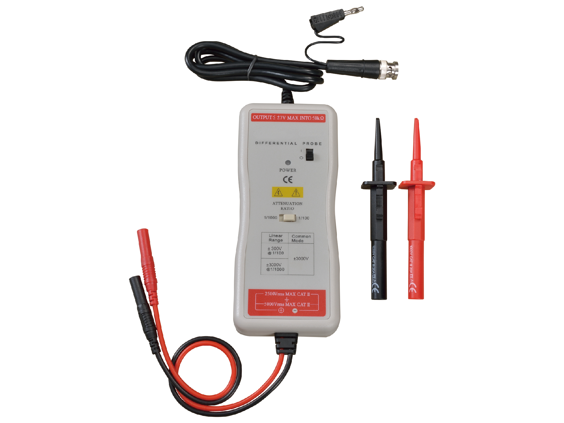
Equipment in this demo: PMK FireFly® FF-1500A · PMK HSDP High-Speed Differential Probe · PMK UFCS Ultra-Fast Current Shunt · PMK MMCX Passive Probe · Iwatsu Digital Oscilloscope · Infineon GaN Half-Bridge Demo Board
All photos: Thomas · @SignalByThomas